MAY 19, 2025
Summer Processing Lab: Week 1 (5/19)
I am participating in the Semiconductor Readiness Organization's Summer Processing Lab. We are gaining hands-on experience with the fundamental techniques that go into Metal Oxide Semiconductor (MOS) capacitor manufacturing. We are not using cleanroom procedures, so our results are expected to be nothing remarkable, but it is great experience regardless.
During our first session, we covered the general procedures and techniques we will be using throughout the summer, and grew the Silicon Oxide layer on our wafers.
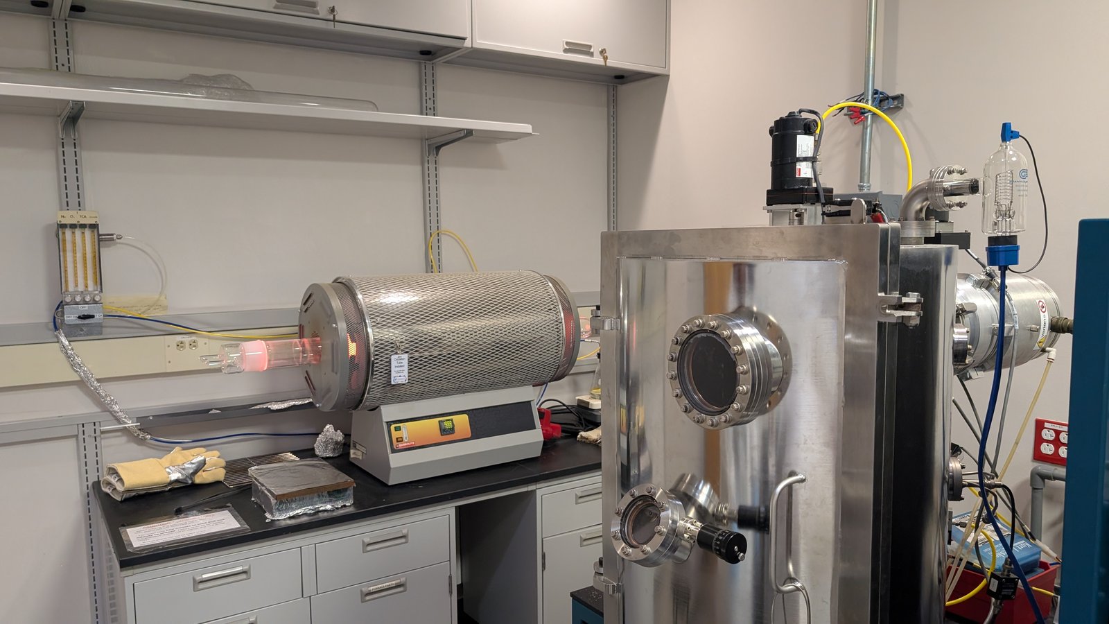
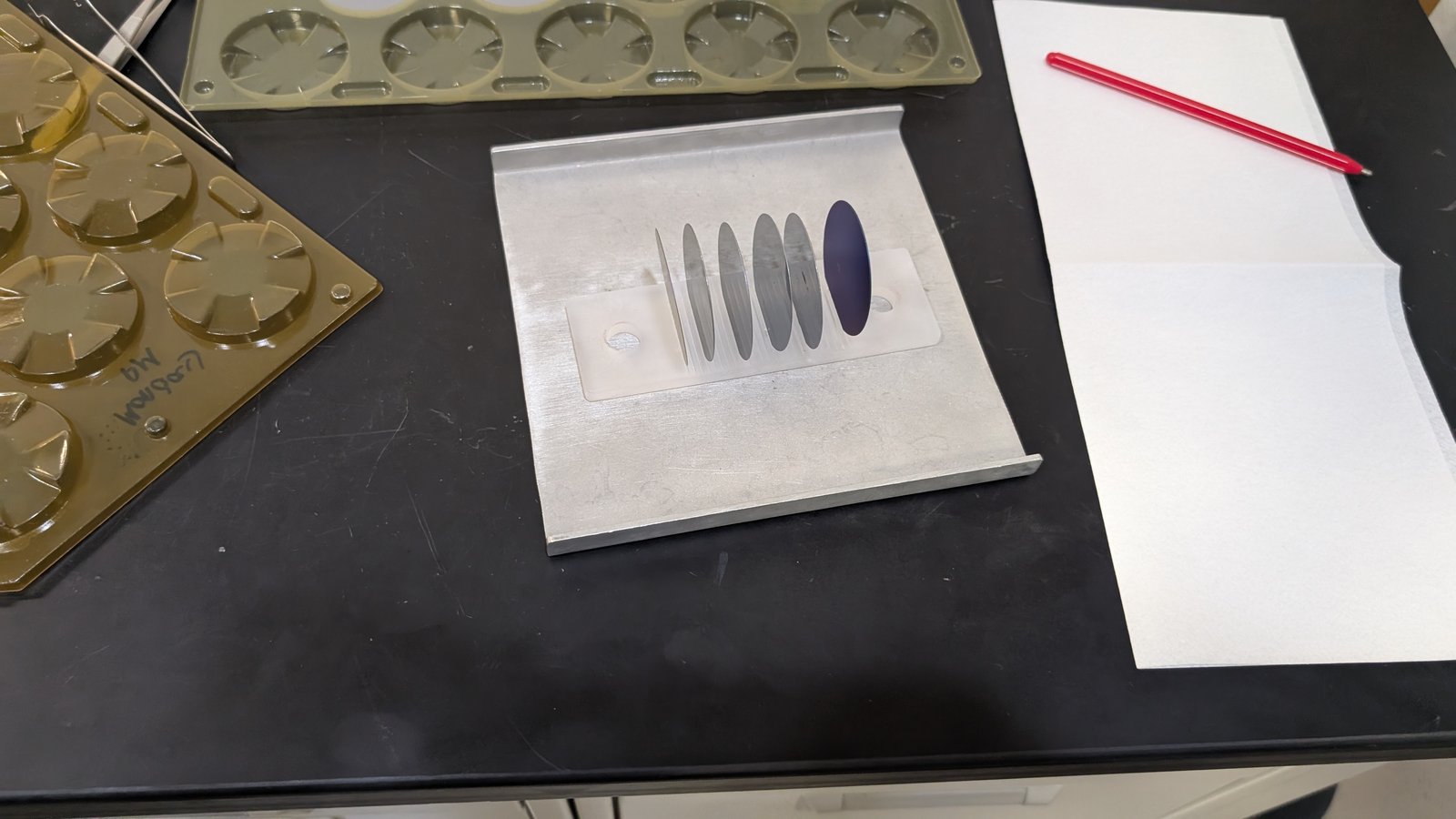
Using the tube furnace at 1000C, we conducted a cycle of dry growth on 4 of the wafers, demarked dry, and wet growth on the remaining 4 wafers, also labelled.